- 您现在的位置:买卖IC网 > Sheet目录19115 > FDP3632 (Fairchild Semiconductor)MOSFET N-CH 100V 80A TO-220AB
�� �
�
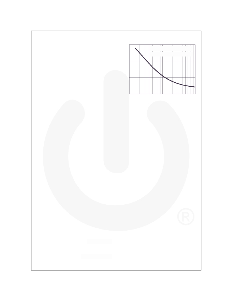
�Thermal� Resistance� vs.� Mounting� Pad� Area�
�The� maximum� rated� junction� temperature,� T� JM� ,� and� the�
�thermal� resistance� of� the� heat� dissipating� path� determines�
�the� maximum� allowable� device� power� dissipation,� P� DM� ,� in� an�
�application.� Therefore� the� application’s� ambient�
�temperature,� T� A� (� o� C),� and� thermal� resistance� R� θ� JA� (� o� C/W)�
�must� be� reviewed� to� ensure� that� T� JM� is� never� exceeded.�
�Equation� 1� mathematically� represents� the� relationship� and�
�serves� as� the� basis� for� establishing� the� rating� of� the� part.�
�80�
�60�
�R� θ� JA� = 26.51+ 19.84/(0.262+Area) EQ.2�
�R� θ� JA� =� 26.51+� 128/(1.69+Area)� EQ.3�
�(� T� –� T� )�
�P� D� M� =� -----------------------------�
�JM A�
�R� θ� JA�
�(EQ.� 1)�
�40�
�In� using� surface� mount� devices� such� as� the� TO-263�
�package,� the� environment� in� which� it� is� applied� will� have� a�
�20�
�significant� influence� on� the� part’s� current� and� maximum�
�power� dissipation� ratings.� Precise� determination� of� P� DM� is�
�complex� and� influenced� by� many� factors:�
�0.1�
�(0.645)�
�1�
�(6.45)�
�AREA,� TOP� COPPER� AREA� in� 2� (cm� 2� )�
�10�
�(64.5)�
�Figure� 21.� Thermal� Resistance� vs� Mounting�
�1.� Mounting� pad� area� onto� which� the� device� is� attached� and�
�whether� there� is� copper� on� one� side� or� both� sides� of� the�
�board.�
�2.� The� number� of� copper� layers� and� the� thickness� of� the�
�board.�
�3.� The� use� of� external� heat� sinks.�
�4.� The� use� of� thermal� vias.�
�5.� Air� flow� and� board� orientation.�
�6.� For� non� steady� state� applications,� the� pulse� width,� the�
�duty� cycle� and� the� transient� thermal� response� of� the� part,�
�the� board� and� the� environment� they� are� in.�
�Fairchild� provides� thermal� information� to� assist� the�
�designer� ’s� preliminary� application� evaluation.� Figure� 21�
�defines� the� R� θ� JA� for� the� device� as� a� function� of� the� top�
�copper� (component� side)� area.� This� is� for� a� horizontally�
�positioned� FR-4� board� with� 1oz� copper� after� 1000� seconds�
�of� steady� state� power� with� no� air� flow.� This� graph� provides�
�the� necessary� information� for� calculation� of� the� steady� state�
�junction� temperature� or� power� dissipation.� Pulse�
�applications� can� be� evaluated� using� the� Fairchild� device�
�Spice� thermal� model� or� manually� utilizing� the� normalized�
�maximum� transient� thermal� impedance� curve.�
�Thermal� resistances� corresponding� to� other� copper� areas�
�can� be� obtained� from� Figure� 21� or� by� calculation� using�
�Equation� 2� or� 3.� Equation� 2� is� used� for� copper� area� defined�
�in� inches� square� and� equation� 3� is� for� area� in� centimeter�
�square.� The� area,� in� square� inches� or� square� centimeters� is�
�the� top� copper� area� including� the� gate� and� source� pads.�
�Pad� Area�
�=� 26.51� +� -----------------� ----� ----------------�
�R�
�θ� JA�
�19.� 84�
�(� 0.262� +� Area� )�
�(EQ.� 2)�
�Area� in� Iches� Squared�
�=� 26.51� +� -----------------� ----� -------------�
�R�
�θ� JA�
�12� 8�
�(� 1.69� +� Area� )�
�(EQ.� 3)�
�Area� in� Centimeter� Squared�
�?� 200� 4� Fairchild� Semiconductor� Corporation�
�FDH3632� /� FDP3632� /� FDB3632� Rev.� C� 5�
�7�
�www.fairchildsemi.com�
�发布紧急采购,3分钟左右您将得到回复。
相关PDF资料
550-5607F
LED 5MM RT ANG SUP CLR GRN PCMNT
ASD3-50.000MHZ-ECT
OSCILLATOR 50.000 MHZ 1.8V SMD
568-0212-222F
LED CBI 4MM 4X1 GRN,GRN,GRN,GRN
ASD3-40.000MHZ-ECT
OSCILLATOR 40.000 MHZ 1.8V SMD
SSF-LXH100HD-01
LED 5MM RA RED DIFF PC MOUNT
564-0140-207F
LED CBI 3MM 3X1 GREEN/X/ORANGE
ASD1-60.000MHZ-ECT
OSCILLATOR 60.000 MHZ 3.0V SMD
76PRB09ST
SWITCH DIP PIANO SEALED 9POS
相关代理商/技术参数
FDP3632_G
制造商:Fairchild 功能描述:TO-220,SINGLE,NCH,100V,99M OHM
FDP3632_NL
制造商:Fairchild 功能描述:100V/80A N-CH MOSFET
FDP3632_Q
功能描述:MOSFET 100V 80a .9 Ohms/VGS=1V
RoHS:否 制造商:STMicroelectronics 晶体管极性:N-Channel 汲极/源极击穿电压:650 V 闸/源击穿电压:25 V 漏极连续电流:130 A 电阻汲极/源极 RDS(导通):0.014 Ohms 配置:Single 最大工作温度: 安装风格:Through Hole 封装 / 箱体:Max247 封装:Tube
FDP3651U
功能描述:MOSFET 100V 80A 15 OHM NCH POWER TREN
RoHS:否 制造商:STMicroelectronics 晶体管极性:N-Channel 汲极/源极击穿电压:650 V 闸/源击穿电压:25 V 漏极连续电流:130 A 电阻汲极/源极 RDS(导通):0.014 Ohms 配置:Single 最大工作温度: 安装风格:Through Hole 封装 / 箱体:Max247 封装:Tube
FDP3652
功能描述:MOSFET 100V 61a 0.016 Ohm RoHS:否 制造商:STMicroelectronics 晶体管极性:N-Channel 汲极/源极击穿电压:650 V 闸/源击穿电压:25 V 漏极连续电流:130 A 电阻汲极/源极 RDS(导通):0.014 Ohms 配置:Single 最大工作温度: 安装风格:Through Hole 封装 / 箱体:Max247 封装:Tube
FDP3652
制造商:Fairchild Semiconductor Corporation 功能描述:MOSFET N TO-220
FDP3652_NL
制造商:Fairchild 功能描述:100V/61A N-CH MOSFET
FDP3652_Q
功能描述:MOSFET 100V 61a 0.016 Ohm RoHS:否 制造商:STMicroelectronics 晶体管极性:N-Channel 汲极/源极击穿电压:650 V 闸/源击穿电压:25 V 漏极连续电流:130 A 电阻汲极/源极 RDS(导通):0.014 Ohms 配置:Single 最大工作温度: 安装风格:Through Hole 封装 / 箱体:Max247 封装:Tube